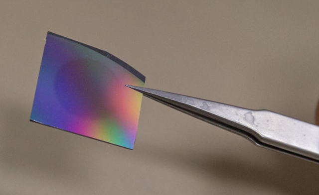
A research group at the National Institute of Nanotechnology (CRNE), in collaboration with researchers at the University of Barcelona's Department of Electronic Engineering, has developed a more convenient and cheaper method of making crystalline silicon. Their research is published in the latest issue of Applied Physics. This very thin silicon wafer is around 10 microns thick and expensive, but what microelectronics expect, especially with the development of microchip 3D integrated circuits, is an inevitable choice. The development of silicon technology provides a broader prospect for the development of photovoltaic technology, especially for the development of flexible batteries. In recent years, the development of technology has brought silicon to the more thin direction. The thinnest wafers that line cutting can bring are about 150 microns thick. It is difficult to obtain thinner wafers by wire cutting, but about half the silicon material that is lost during the cutting process. The team's approach differs from that of conventional wire sawing in that it takes only one step to achieve and produces more efficient, faster, and cheaper silicon wafers. The method is based on the surface of the material to create a lot of tiny pores, processing assisted high temperature to achieve. The silicon wafer segmentation process precisely controls the shape of tiny pores. Precise control of the pore diameter not only controls the number of wafers, but also allows for precise control of thickness as well as tolerances. This sandwich-like wafer can be flaked off. The expected number and thickness of wafers can be controlled very accurately. CRNE scientists can easily slice a 300-mm thick piece of silicon into 10 thinner pieces of silicon, each measuring between 5 and 7 millimeters. Reduce the cost of industrial production The demand for ultra-thin silicon is increasing, both in the MEMES and in the solar industry. Cutting the traditional silicon has reached a relative bottleneck stage. The thickness of silicon wafers ranges from 300 millimeters in the 1990s to around 180 millimeters nowadays, and the efficiencies are continuously increasing and costs are reduced, but the desire to obtain thinner wafers to further reduce costs is becoming more and more difficult. The advent of this approach addresses this need well, despite the tens of microns of thickness, but the ability to absorb and convert sunlight is maintained. Traditional Transformer Ac Arc Welder Traditional Transformer Ac Arc Welder,Transformer Ac Arc Welding Machine,Arc Transformer Welding Machine Songshi Electric Appliance Factory , http://www.ykweldingmachine.com