WinnerLifting supplies both Single Stud Fittings and Double Stud Fittings.
And there are even non-standard multiple stud fittings.
All these End Fittings are accessories of certain Ratchet Straps,they are acting like anchor point with matched tracks.
Cargo control field is a big world,there are always something waiting for you to explore.
Reach us for more detail,thank you!
Single Stud Fittings Single Stud Fittings,Recessed Lashing Rings,Mounting Ring Flush,Cargo Control Fitting,Stud Fitting WINNERLIFTING(H.K.)INT'L TRADING LIMITED. , https://www.massagebeds.nl
The process of chip manufacturing is like building a house with Lego. After first wafers are used as foundations and then stacked up, the necessary IC chips can be produced (which will be described later). However, without a blueprint, it is useless to have a strong manufacturing capability. Therefore, the role of the architect is very important. But who is the architect in IC design? This article next describes IC design.
In the IC production process, ICs are mostly planned and designed by professional IC design companies. For example, MediaTek, Qualcomm, Intel, and other famous manufacturers all design their own IC chips and provide chips of different specifications and performance to downstream manufacturers. Because ICs are designed by each company, IC design relies on engineers' skills. The quality of engineers affects the value of a company. However, what steps do engineers have when designing an IC chip? The design process can be simply divided into the following. 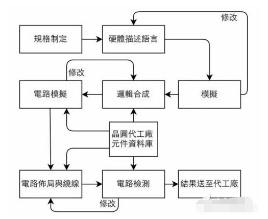
Designing the first step and setting goals
The most important step in IC design is specification. This step is like deciding on a few rooms and bathrooms before designing a building. There are building regulations that need to be followed, and the design is done after all the functions have been determined so that no additional time is needed for subsequent modifications. The IC design also needs to go through similar steps to ensure that the designed chip will not have any errors.
The first step in specification development is to determine the purpose and effectiveness of the IC and to set the general direction. The next step is to see which protocols are to be complied with. A chip like a wireless network card needs to comply with the IEEE 802.11 standard. Otherwise, the chip will not be compatible with the products on the market, making it impossible to connect with other devices. The last step is to establish the implementation method of this IC, allocate different functions into different units, and establish the connection method between different units, thus completing the specification.
After designing the specifications, the design details of the chip are then followed. This step is like taking a preliminary note of the building's plan and depicting the overall outline to facilitate subsequent drawing. In an IC chip, a circuit is described using a hardware description language (HDL). Frequently used HDLs are Verilog, VHDL, etc., and one IC function can be expressed easily by using code. The next step is to check the correctness of the program's functionality and continue to modify it until it meets the desired functionality. 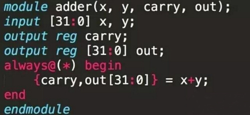
With computers, everything becomes easy
With the complete plan, the next step is to draw a blueprint for the design. In IC design, this step of logic synthesis is to put the HDL code that is unmistakable into the electronic design automation tool (EDA tool), and let the computer convert the HDL code into a logic circuit to generate the following circuit diagram. After that, it is determined repeatedly whether the logic gate design conforms to the specifications and changes until the function is correct. 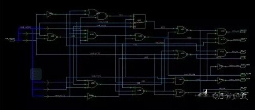
Finally, the synthesized code is put into another set of EDA tool for circuit layout and placement (Place And Route). After continuous testing, the following circuit diagram will be formed. Different colors such as blue, red, green and yellow can be seen in the figure, and each different color represents a mask. As for how to use the mask? 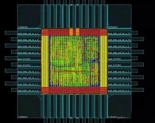
Layer masks, stacking a chip
First of all, it is known that an IC will generate multiple masks. These masks have upper and lower layers, and each layer has its own task. The following figure shows a simple photomask example. Taking the most basic component CMOS in an integrated circuit as an example, CMOS is named full complement metal-oxide-semiconductor (NMOS and PMOS). Combine to form CMOS. What is a metal oxide semiconductor (MOS)? This kind of device that is widely used in the chip is more difficult to explain, and it is more difficult for ordinary readers to clarify.
In the figure below, the left side is the circuit diagram after circuit layout and winding. It is known in the front that each color represents a mask. On the right is how each photo mask spreads out. The production process starts with the bottom layer and follows the method mentioned in the last IC chip manufacturing process. It will be produced layer by layer, and finally the desired chip will be produced. 
At this point, there should be a preliminary understanding of IC design. As a whole, it is clear that IC design is a very complicated profession. Thanks to the maturity of computer-assisted software, IC design can be accelerated. The IC design factory relies heavily on the wisdom of the engineers. Each step described here has its own specific knowledge and can be independently integrated into multiple professional courses. For example, writing a hardware description language is not simply a matter of knowing the programming language. You also need to understand how logic circuits work, how to convert the required algorithms into programs, and how the synthesis software converts programs into logic gates.
Among the major semiconductor design companies are Intel, Qualcomm, Broadcom, Infinity, Happy, Xilinx, Altera, MediaTek, Hass, Spreadtrum, ZTE Microelectronics, Huada, Datang, Zhixin, Duntai, Silan, and China Star. , etc.
What is a wafer?
In semiconductor news, there are always mentions of wafer factories that are marked with dimensions, such as 8-inch or 12-inch fabs. However, what is the so-called wafer in the end? Which part of the 8 inch refers to? What is the difficulty in producing large-size wafers? The following is a step-by-step introduction to the most important foundation of semiconductors - what exactly is a "wafer."
Wafers are the foundation for making all kinds of computer chips. We can compare chip manufacturing to building houses with Lego bricks, stacking layers one by one to complete our own desired style (ie, various types of chips). However, if there is no good foundation, the covered house will squat around. It is not what you want. In order to make a perfect house, you need a smooth base plate. For chip manufacturing, this substrate is the wafer that will be described next. 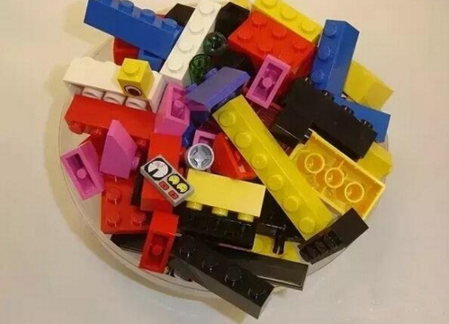
First of all, first recall that when a child was a Lego building block, the surface of the building blocks would have a small round projection. With this construction, we could stack the two building blocks stably without using glue. . Chip fabrication also fixes the subsequently added atoms and substrates in a similar manner. Therefore, we need to find a substrate with a neat surface to meet the requirements for subsequent manufacturing.
In solid materials, there is a special crystal structure - Monocrystalline. It has the characteristics of atoms arranged one after the other, forming a flat surface of atoms. Therefore, the use of single crystal wafers can meet the above needs. However, there are two main steps in how to produce such materials, namely, purification and pulling, and then such materials can be completed.
How to make a single crystal wafer <br> <br> purified in two stages, the first step is purification of metallurgical grade, this process is mainly added to the carbon, in a redox manner, converted into silicon oxide 98% purity Silicon. Most of the metals extracted, such as iron or copper, are obtained in such a way that they are of sufficient purity. However, 98% is still not enough for chip manufacturing and still needs further improvement. Therefore, Siemens process will be further used for purification. In this way, high-purity polysilicon required for semiconductor process will be obtained. 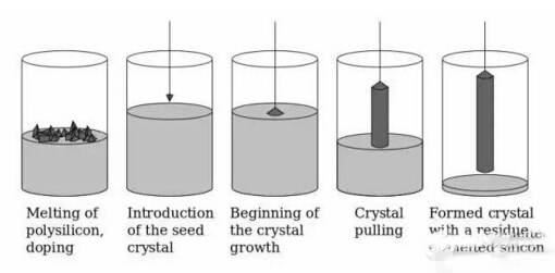
Then, it is the step of pulling crystals. First, the high purity polysilicon previously obtained is melted to form liquid silicon. After that, the single-crystal silicon seed is brought into contact with the surface of the liquid and slowly pulled up while rotating. As to why single-crystal silicon is needed, it is because the arrangement of silicon atoms is the same as that of people. They will need to be ranked first so that people can correctly arrange them. Silicon is the important leader, and later atoms know how to line up. Finally, after the silicon atoms leaving the liquid surface solidify, the aligned single crystal silicon column is completed. 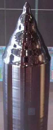
However, what does 8 inch and 12 inch represent? He refers to the crystal column that we have produced, the part that looks like a pencil pen, and the diameter of the surface that has been processed and cut into thin wafers. As for the difficulty of manufacturing large-size wafers? As mentioned earlier, the manufacturing process of the crystal column is like forming marshmallows, and it is molded while rotating. If you have made marshmallows, you should all know that it is very difficult to make big and solid marshmallows, and the same is true for pulling crystals. The speed of pulling and the temperature control will affect the quality of the crystal column. As a result, the larger the size, the higher the speed and temperature requirements for pulling crystals, so the difficulty of making high-quality 12-inch wafers is still higher for 8-inch wafers.
However, an entire silicon pillar cannot be made into a chip-manufactured substrate. In order to produce a single silicon wafer, a silicon knife is then required to cut the silicon crystal pillar laterally into a wafer. The wafer can then be formed by polishing. Make the required silicon wafers. After so many steps, the manufacturing of the chip substrate is completed, and the next step is the step of stacking the house, that is, the chip manufacturing. As for how to make a chip?
Stacked chips
After introducing what silicon wafers are, it is also known that manufacturing IC chips is like building a house with Lego bricks, creating layers of layers to create their own desired shapes. However, there are quite a few steps to building a house. IC manufacturing is the same. What steps are there to make an IC? This article will introduce the process of IC chip manufacturing.
Before we begin, we must first understand what the IC chip is. The IC, the full name Integrated Circuit, is known by its name as a circuit that is designed to be assembled in a stacked manner. With this method, we can reduce the area required to connect the circuit. The following figure shows the 3D diagram of the IC circuit. From the figure, it can be seen that its structure is like that of the house and the column, stacked one above the other, which is why the IC manufacturing will be compared to building a house. 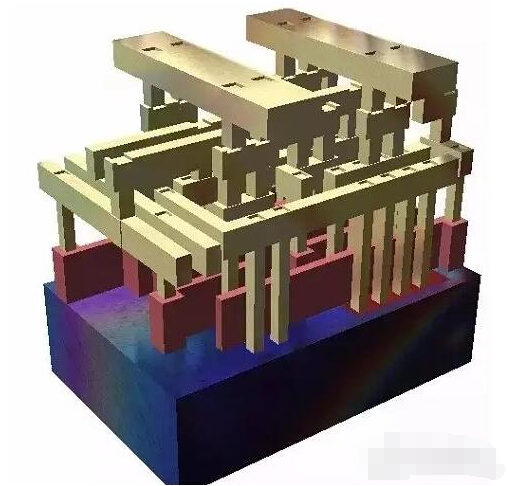
From the 3D cross-sectional view of the IC chip in the figure above, the dark blue part at the bottom is the wafer introduced in the previous article. From this figure, we can more clearly know how important the wafer substrate plays a role in the chip. As for the red and khaki-colored parts, it is where the ICs are to be manufactured.
First of all, here we can compare the red part to the first floor lobby in a tall building. The lobby on the first floor is the gateway to a house. This is where the traffic comes in and out. It usually has more functions under the control of traffic. Therefore, when compared with other floors, it will be more complex and require more steps. In the IC circuit, this hall is the logic gate layer, which is the most important part of the entire IC. By combining multiple logic gates together, a fully functional IC chip is completed.
The yellow part is like an ordinary floor. Compared with the first floor, there will be no complicated structures, and there will not be much change in each floor when it is built. The purpose of this layer is to connect the logic gates of the red part. The reason why so many layers are needed is because there are too many lines to be linked together. In a single layer that cannot accommodate all the lines, it is necessary to build several layers to achieve this goal. Among these, the lines of different layers are connected up and down to meet the wiring requirements.
Layered construction, layer by layer architecture
After knowing the structure of the IC, the next step is to describe how to make it. Imagine if we want to do a fine picture with a paint sprayer, we need to cut out the graphic cover and cover it on paper. Then spray the paint evenly on the paper. After the paint is dry, remove the mask again. Repeatedly repeating this step will complete the neat and complex graphics. The ICs are manufactured in a similar manner, stacked one on top of the other in a masked manner. 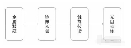
When making ICs, you can simply divide the above 4 steps. Although the actual manufacturing process differs in the manufacturing steps and the materials used are different, similar principles are generally adopted. This process is a little different from paint painting. IC manufacturing is the first paint to cover, and paint painting is to cover and paint. The following describes the various processes.
Metal Sputtering: The metal material to be used is uniformly sprinkled on the wafer to form a thin film.
Coating photoresist: The photoresist material is placed on the wafer first, passes through the reticle (the mask principle is left for the next explanation), and the beam is hit on the unnecessary part to destroy the structure of the photoresist material. Then, the chemical is used to wash away the damaged material.
Etching: Silicon wafers that are not protected by photoresist are etched with ion beams.
Photoresist removal: The photoresist remaining in the photoresist is dissolved and this completes the process.
In the end, a lot of IC chips will be completed on a whole wafer. As long as the finished square IC chips are cut off, they can be sent to the packaging factory for packaging. What is the packaging factory? It will be followed by instructions. 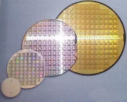
Among them, major foundries are Groovy, Samsung Electronics, Tower Jazz, Dongbu, Magna, IBM, Fujitsu, Intel, Hynix, TSMC, UMC, SMIC, Powerchip, Hua Hong, De Mao Wuhan Xinxin, Hua Wei, Holley, force core <br> <br> nanometer process what is?
Samsung and Taiwan Semiconductor Manufacturing Co., Ltd. are playing very hot on advanced semiconductor manufacturing processes. They both want to grab an opportunity to win orders in the wafer foundry. It is almost a competition between 14nm and 16nm, but 14nm and 16nm respectively. What is the meaning of the number and what part is it referring to? What benefits and problems will it bring in the future after narrowing the process? In the following, we will give a brief explanation of the nanometer process.
How fine is nano?
Before you begin, understand what nanotechnology really means. In mathematics, the nanometer is 0.000000001 meters, but this is a very bad example. After all, we only see that there are many zeros after the decimal point, but there is no actual feeling. If you compare the thickness of nails, it may be more obvious.
Actually measured with a ruler, it can be seen that the thickness of the nail is about 0.0001 meters (0.1 mm), that is, try to cut the side of a nail into 100,000 lines, each line is equivalent to about 1 nanometer. This can be slightly imagined how tiny 1 nanometer is.
After knowing how small the nanometers are, they also need to understand the intention of narrowing down the process. The main purpose of reducing the size of transistors is to insert more transistors into smaller chips so that the chips will not become more advanced due to technological improvements. Large; second, can increase the processor's computing efficiency; Moreover, reducing the size can also reduce power consumption; Finally, after the chip size is reduced, it is easier to stuff into the mobile device to meet the future needs of thin and light.
Let's go back and explore what is the nanometer process. Take 14nm as an example. The process is the minimum size of the line can be 14nm in the chip. The figure below shows the longitude of the conventional transistor, as an example. The main purpose of reducing the transistor is to reduce the power consumption. However, which part should be reduced to achieve this goal? The L in the image on the left is the part we want to shrink. By reducing the gate length, the current can be routed from Drain to Source with a shorter path (if you are interested, you can use Google to search for MOSFETs, which will be explained in more detail). 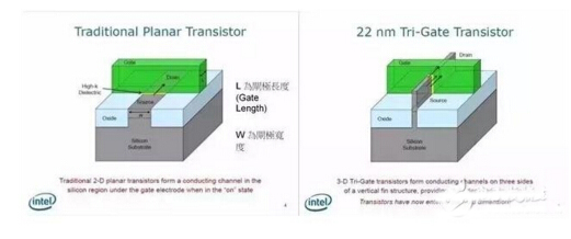
In addition, the computer is based on 0 and 1 operations. How do we use transistors to meet this goal? The practice is to determine whether the transistor has current flow. When the voltage is supplied to the Gate terminal (green box), the current will flow from the Drain terminal to the Source terminal. If no voltage is supplied, the current will not flow, so that 1 and 0 can be represented. (As to why you should use 0 and 1 as a judgment, if you are interested, you can go to Chablin algebra. We use this method to make a computer.)
Size reduction has its physical limitations
However, the process can not be unlimitedly reduced. When we shrink the transistor to about 20 nanometers, we will encounter problems in quantum physics, so that the transistor has leakage phenomenon, offsetting the benefits obtained by reducing the L. As an improvement, the concept of Fin FET (Tri-Gate) is introduced, as shown in the top right figure. In Intel's previous explanation, it can be understood that by introducing this technology, leakage due to physical phenomena can be reduced. 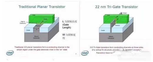
More importantly, this method can increase the contact area between the Gate and the lower layer. In the traditional practice (above left), the contact surface has only one plane, but after using Fin FET (Tri-Gate) technology, the contact surface will become three-dimensional, and the contact area can be easily increased, so that the same can be maintained. Making the Source-Drain end smaller under the contact area is a great help in reducing the size.
Finally, why would anyone say that the major plants will face considerable challenges when they enter the 10-nanometer process, mainly because the size of a single atom is about 0.1 nanometers, and in the case of 10 nanometers, a line has less than 100 atoms, It is very difficult to produce, and if there is an atomic defect, such as an atom falling out or impurities in the production process, it will produce an unknown phenomenon, affecting the yield of the product.
If you can't imagine this difficulty, you can do a little experiment. On the table, use 100 beads to arrange a 10×10 square, and cut a piece of paper to cover the beads. Then use a small brush to brush the next bead and finally make him a 10×5 rectangle. In this way, we can know the difficulties faced by major plants and how difficult it is to achieve this goal.
As Samsung and Taiwan Semiconductor Manufacturing Co. Ltd. will complete mass production of 14-nm and 16-nm FinFETs in the near future, both want to compete for Apple’s next-generation iPhone chip foundry. We will see great business competition, and we will also get more power. , thin mobile phones, thanks to the benefits brought by Moore's Law.
Tell you what is package
After a long process, from design to manufacturing, an IC chip was finally obtained. However, a chip is quite small and thin. If it is not applied outside, it will be easily scratched and damaged. In addition, because of the tiny size of the chip, it would not be easy to manually place on a circuit board without using a larger size housing. Therefore, this article next describes the package description.
At present, there are two kinds of common packages, one is common in the electric toy, the black looks like a dip in a DIP package, and the other is a common BGA package when buying a boxed CPU. As for other packaging methods, there are PGAs (Pin Grid Array; Pin Grid Array) used in earlier CPUs or DIPs improved QFPs (Plastic Quad Flat Packings). Because there are too many packaging methods, the following will introduce the DIP and BGA packages.
Traditional packaging, enduring
The first thing to introduce is the Dual Inline Package (DIP). From the figure below, you can see that the IC chip with this package looks like a black bar under the double row of pins, which is very impressive. The packaging method is the earliest IC packaging technology and has the advantage of low cost. It is suitable for small chips that do not require too many wires. However, because most plastics are used, the heat dissipation effect is poor and cannot meet the requirements of current high-speed chips. Therefore, most of the chips that use this package are enduring chips, such as the OP741 in the figure below, or IC chips that are not required for the operation speed and have smaller chips and fewer contacts. 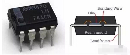
As for the Ball Grid Array (BGA) package, the package size is smaller than that of the DIP and can be easily put into a smaller device. In addition, because the pin is located below the chip, the more metal pins that can be accommodated than the DIP are quite suitable for chips that require more contacts. However, the use of such a packaging method has a high cost and a complicated connection method, and is therefore mostly used in high-priced products. 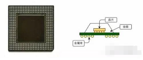
The rise of mobile devices, new technology has leapt to the stage <br> <br> However, use of these packaging method, will spend out considerable volume. The current mobile devices, wearable devices, etc., require a large number of components. If the individual components are individually packaged, the combination will consume a very large space. Therefore, there are currently two methods that can meet the requirements for reducing the size. These are SoCs ( System On Chip) and SiP (System In Packet).
When the smart phone first emerged, the term SoC could be found in various financial miscellaneous items. However, what is SoC? In simple terms, ICs with different functions are integrated into one chip. With this method, not only can the size be reduced, but also the distance between different ICs can be reduced and the calculation speed of the chip can be increased. As for the production method, it is during the IC design stage that various ICs are put together and then a mask is created through the previously described design flow.
However, the SoC is not only an advantage. To design a SoC requires a considerable amount of technical cooperation. When the IC chips are individually packaged, each package has external protection, and the distance between the IC and the IC is relatively long, and no interaction interference occurs. However, when all ICs are packaged together, it is the beginning of a nightmare. The IC design factory will change from simply designing ICs to ICs that understand and integrate each function, and increase the workload of engineers. In addition, there are many situations in which high-frequency signals such as communication chips may affect other functions such as ICs.
In addition, SoCs also need to obtain the IP (intellectual property) authorization from other vendors in order to put components designed by Others into the SoC. Because the SoC needs to obtain the design details of the entire IC, a complete mask can be made, which also increases the design cost of the SoC. Some people may question why not design one yourself? Because designing various ICs requires a great deal of knowledge related to this IC, only companies with a lot of money like Apple can budget to excavate top engineers from well-known companies to design a brand-new IC through cooperative authorization or more than their own. More research and development cost-effective.
Eclectic solution, SiP appeared
As an alternative, SiP jumped onto the stage of integrating chips. Unlike the SoC, it is the purchase of various ICs. The last time these ICs are packaged, this reduces the IP licensing step and drastically reduces design costs. In addition, since they are separate ICs, the degree of interference with each other has dropped significantly. 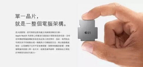
Products using SiP technology, the most famous non-AppleWatch must be. Because Watch's internal space is too small, it cannot adopt the traditional technology, the design cost of SoC is too high, SiP becomes the first choice. With SiP technology, not only can the size be reduced, but the distance between ICs can also be narrowed down to become a feasible compromise solution. The following figure shows the structure of the Apple Watch chip. You can see that quite a few ICs are included. 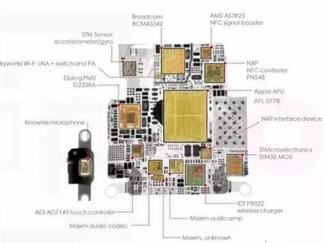
After the package is completed, it is necessary to enter the test phase. At this stage, it is necessary to confirm whether the packaged IC is operating normally. After correctness, the packaged product can be shipped to the assembly plant to make the electronic products we have seen. Among the major semiconductor packaging and testing companies are Ansico, Starcore, J-devices, Unisem, Nepes, Riyueguang, Licheng, Nanmao, Shan State, Jingyuan Electronics, Fushen, Lingsheng Precision, Xipin, Changdian, Youte
Complex and cumbersome chip design flow
Verilog example of 32bits adder.
Control unit synthesis results.
Commonly used calculation chip - FFT chip, complete the circuit layout and winding results.
(Souse: Flickr/Jonathan Stewart CC BY 2.0)
Silicon column manufacturing process (Source: Wikipedia)
Monocrystalline column (Souse: Wikipedia)
3D profile of an IC chip. (Source: Wikipedia)
Comparison of wafers of various sizes. (Source: Wikipedia)
(Source: share.net)
(Source: share.net)
The IC chip on the left is the OP741, which is a common voltage amplifier. The figure on the right shows its sectional view. This package connects the chip to the metal lead frame with a gold wire. (Source: Wikipedia on the left and Wikipedia on the right)
The figure on the left shows the chip in BGA package. The figure on the right shows a BGA schematic using a flip-chip package. (Source: Wikipedia, left)
Apple Watch uses SiP technology to encapsulate the entire computer architecture into a single chip, not only satisfying the desired performance but also reducing the size, allowing the hand to have more room to put the battery. (Source:Apple)
The SiP packaged S1 chip internal configuration diagram is used in the Apple Watch. (Source:chipworks)