First, the working principle of
solar cells
A solar cell is a pair of devices that respond to light and convert light energy into electricity. There are many kinds of materials that can produce photovoltaic effect, such as: monocrystalline silicon, polycrystalline silicon, amorphous silicon, gallium arsenide, selenium indium copper, and the like. Their power generation principles are basically the same. Now, crystalline silicon is taken as an example to describe the photovoltaic power generation process. P-type crystalline silicon is doped with phosphorus to obtain N-type silicon to form a PN junction.
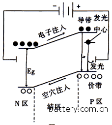
When the light illuminates the surface of the solar cell, part of the photons are absorbed by the silicon material; the energy of the photons is transferred to the silicon atoms, causing the electrons to move more and more, and the free electrons accumulate on both sides of the PN junction to form a potential difference. When the circuit is turned on, under the action of this voltage, a current will flow through the external circuit to generate a certain output power. The essence of this process is the process of converting photon energy into electrical energy.
Second, the production process of solar cells
Rich in silicon
"Silicon" is one of the most abundant materials on our planet. Since the discovery of the semiconductor properties of crystalline silicon in the 19th century, it has changed almost everything, even human thinking. At the end of the 20th century, the role and role of “silicon†can be seen everywhere in our lives. Crystalline silicon solar cells have become the fastest industrialized in the past 15 years.
production process
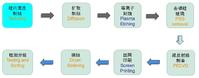
The production process can be roughly divided into five steps: a, purification process b, draw bar process c, slicing process d, battery process e, and packaging process.
Taking monocrystalline silicon as an example, its production process can be divided into:
Process one, silicon wafer cleaning and velvet
Purpose - surface treatment:
Remove surface oil and metal impurities;
Removing a cutting damage layer on the surface of the silicon wafer;
Making a suede on the surface of the silicon wafer to form an anti-reflective texture to reduce the surface reflectance;
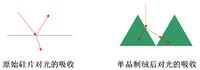
Using the anisotropic etching of Si in dilute NaOH solution, a pyramid structure of 3-6 microns is formed on the surface of the silicon wafer, so that the light is reflected and refracted multiple times on the surface of the silicon wafer, which increases the absorption of light;
Process 2, diffusion
The single/double-sided liquid source of the silicon wafer is diffused to form an N-type emitter region to form a basic structure for photoelectric conversion: a PN junction.
POCl3 liquid molecules enter the furnace tube under the carrier of N2 carrier gas, and are replaced by a series of chemical reaction phosphorus atoms at high temperature, diffused into the surface of the silicon wafer, activated to form N-type doping, and form a PN junction with the P-type substrate. The main chemical reactions are as follows:
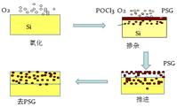
POCl3 + O2 → P2O5 + Cl2 P2O5 + Si → SiO2 + P
Process three, plasma engraving
Removing the short circuit ring formed around the silicon wafer after diffusion;
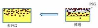
Step 4, removing the phosphorus silicon glass
The surface of the silicon wafer is removed and the phosphosilicate glass formed during diffusion (phosphorus silica glass refers to a SiO2 layer doped with P2O5).
Process 5, PECVD
Purpose - anti-reflection + passivation:
PECVD, plasma enhanced chemical vapor deposition equipment, Plasma Enhanced Chemical Vapor Deposition;
Making a SiN film (~80 nm) that reduces the surface reflection of the silicon wafer;
The SiN film contains a large amount of hydrogen ions, and hydrogen ions are implanted into the silicon wafer to achieve surface passivation and bulk passivation, which effectively reduces the recombination of carriers and improves the short-circuit current and open circuit voltage of the battery.
Process principle:
The silane reacts with ammonia to form SiN, which is deposited on the surface of the silicon wafer to form an anti-reflection film.
A technique for generating a plasma to affect a chemical vapor deposition process by using a high-frequency power source glow discharge. Due to the presence of plasma, the decomposition, compounding, excitation and ionization of gas molecules are promoted, and the formation of reactive groups is promoted, thereby lowering the deposition temperature. PECVD forms a film in the range of 200 ° C to 500 ° C, which is much smaller than other CVD films in the range of 700 ° C to 950 ° C.
During the reaction, a large amount of hydrogen ions are injected into the silicon wafer, so that the dangling bonds in the silicon wafer are saturated, the defects are deactivated, and the surface passivation and bulk passivation are achieved.
Process six, screen printing
The method of screen printing is used to complete the fabrication of the back field, the back electrode and the positive grid line electrode, and the generated photo-generated current has been extracted;
Process principle:
Printing a certain pattern of silver paste or aluminum paste on the surface of the silicon wafer, forming an ohmic contact after sintering, so that the current is effectively output;
The front electrode is made of Ag metal paste, which is usually printed in a grid line shape to achieve good transmittance while achieving good transmittance.
The back side is usually printed with the entire surface of the Al metal paste, one to overcome the resistance caused by the series connection of the battery, and the other is to reduce the composite of the back side;
Process 7, drying and sintering
Purpose and working principle:
Dry the metal slurry and volatilize the additives (the first 3 zones);
Forming an aluminum-silicon alloy and a silver-aluminum alloy on the back side to make a good back contact (the middle 3 zones);
The Al-Si alloy process is actually a process of P-doping silicon, which needs to be heated to a eutectic point (577 ° C) or higher. After alloying, as the temperature drops, the liquid
The silicon in the phase will re-solidify to form a crystalline layer containing a small amount of aluminum, which compensates for the donor impurities in the N layer, thereby obtaining a P layer with aluminum as the acceptor impurity, thereby achieving the purpose of eliminating the back junction.
Forming a silver-silicon alloy on the front side with good contact and shading rate;
The glass additive in the Ag slurry is fired through the SiN film at a high temperature (~700 degrees), so that the Ag metal contacts the surface of the silicon wafer and is alloyed at a silver-silicon eutectic point (760 degrees) or higher.
Battery Electrolyte
Battery Electrolyte,Trifluoromethanesulfonimide White Powder,Cas 82113-65-3,Trifluoromethanesulfonimide Cas 82113-65-3
Henan Tianfu Chemical Co.,Ltd , https://www.hnphotoinitiators.com